Interferometers
Introduction
You can only make a dish antenna so big. Physically, this is a true statement. The limit is about 100 metres in diameter, if you could afford to engineer the precision metalwork across an area that large, hold it down with enough concrete so it didn't blow away in a storm and be able to steer it and focus where you wanted to observe. Fortunately, there is an alternative method of enlarging the effective aperture of a radio telescope. It's called synthesis imaging interferometry. These instruments can be large, complex and expensive such as the Long Baseline Arrays operated by government research agencies around the world. They can also be small, simple and inexpensive created by clever individuals.
Our High Frequency Interferometer Project
We are currently planning and building a multisite, multiuser, high frequency interferometer (HFI). The HFI will be somewhere between the two examples given in the previous paragraph. The sites will be remote from each other, using an advanced software defined receiver which is phase locked to all receivers in the network with GPS common view techniques. Some sites will be located off the mains grid so efficient hardware and support infrastructure will be used to reduce power consumption, where possible. This will probably mean that only data collection will be carried out at each site, correlation and processing will be carried out at a central facility.
- HFI Design Goals
HFI Design Goals
Fri, 05/28/2010 - 18:33 — peter
Site Network
- Initial Antenna Configuration: Phased Dipole Array
- Alternate antenna configurations: Steered Yagi or log periodic
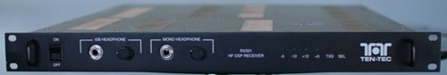
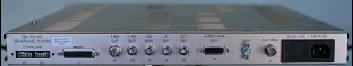
- Receiver OEM & Model: Ten-Tec RX-331 HF DSP Receiver
- Receiver Operating Frequencies:0MHz to 22MHz
- Receiver Operating Bandwidth: 100Hz to 16kHz
- Output data format: Uncompressed audio format (wav.files)
- GPS Disciplined Oscillator OEM & Model: Trimble Thunderbolt
- NTP control: Direct control by GPS Disciplined Oscillator
- Data collection PC: Operating System and data storage on solid state hard drives or memory cards
- Data transfers: High speed internet
- Common View control: High speed internet
Offsite Network Control
- Storage Capacity: sufficient to hold & allow efficient data processing
- Processing Speed: adequate for correlation tasks and fast fourier transforms of data
- Remote control: Access site network for data transfers and configuration changes
HFI Network Sites
- Sat, 06/12/2010 - 21:30 — peter
Receiver sites
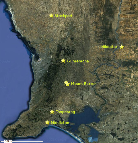
- The following areas outside of the Adelaide metropolitan area are potential network sites for the HFI, this allows us a choice of east-west baselines between approx. 1.5km and 90km in length. Two are observatory sites used by ASSA for optical astronomy and the remainder are private properties owned by ASSA members interested in radio astronomy. There are several suburban sites available to the group that have not been included at this stage of the HFI planning process.
HFI Receivers
Sat, 06/05/2010 - 22:01 — peter
Choice of Receiver for the HFI
The Ten-Tec RX-331 HF DSP Receiver has been chosen as the analog/digital conversion receiver for the HFI for the following reasons:
- Wide bandwidth (16kHz) and good sensitivity for a commercial HF communications receiver
- External 10MHz frequency reference locking capability
- Multidrop RS-232 communication capability
- Choice of outputs and output formats for additional DSP opportunities/capabilities
- Comprehensive documentation is available on the internet here
- Some ASSA members have operational and programming experience with this receiver
- Multiple receivers were available to buy at the time of purchase
- (and finally) they were a good choice for the price
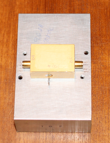
20MHz Low Noise Amplifier
Mon, 11/30/2009 - 21:42 — peter
Introduction
The 20MHz Low Noise Amplifier (LNA) project was begun to help increase the sensitivity of receivers being used for the reception of Jovian Radio Emissions, primarily for users of single dipole antennas. The single dipole is commonly used where space is limited but lower gain is achieved compared to the phased dual dipole arrays which require a significantly greater area to implement.
Having said that, a pair of LNAs fitted to a phased array may increase it's system sensitivity as well.
An additional benefit of using an LNA is to remove the requirement to use tuned lengths of coaxial cable between the antenna and receiver. The output impedance of the LNA can be matched to either a 50Ω or 75Ω input impedance of the receiver.
Primary design goals
The basic design of the LNA is derived from work done by Rick Campbell (KK7B) as part of the R1, R2 and Mini R2 direct conversion receivers, and further developed by others over several years and in particular, Craig Johnson AA0ZZ and Gary Johnson WB9JPS. http://cbjohn.com/aa0zz/
This derivative has the following features:
- centre frequency of 20.1MHz and a bandpass of 4MHz.
- overall +14dB of gain and a noise figure of <5.0
- careful selection of hi-Q components with optimal PCB placement.
- small package located directly at the antenna feedpoint.
- modification of the centre frequency, gain and output impedance are easily made by selection of a few key components at the time of assembly.
Possible Improvements
Currently at the prototype stage and prior to a production run in early 2011, some possible improvements that could be made include:
- replacement of the T05 package, 2N5109 with a suitable SMD alternate.
- re-bias the whole circuit to suit a lower DC voltage: +9V from a rechargeable PP3 battery.
- better coupling for the DC power feed into the circuit. See a possible solution
Schematic Diagram
The schematic has been drawn using gEDA Schematic Editor and saved here as a text file. Similarly, gEDA Attribute Editor has been used to manage the Bill of Materials (BOM). The current version of the gEDA suite is available from the following link. www.gpleda.org/
PCB Layout
The layout has been drawn using PCB Designer and saved here as a text file, the majority of component dimensions and outlines taken from the pcblib-newlib library. The board is cut to fit into a Jaycar Cat No. HB6030, ABS plastic case - 90mm(L) x 50mm(W) x 16mm(H) with full epoxy encapsulation. The torroid inductors are meant to be set into the board to save height and allow better (shorter & symmetrical) lead insertion onto the board. Tuning capacitors have been selected from the American Technical Ceramics (ATC) range and are relatively large, you could swap in regular 1210 or 1206 size components without much trouble, if required. Vias to ground are directly connected through the board to each resistor and capacitor pad rather than along tracks, minimising stray inductances where possible. An SMA jack at one end of the case serves as the amplified signal output to the receiver, the antenna feed wires connect by soldering directly to the dipole elements from the other end.
Simulation and Modeling
No attempt at Spice simulation or similar modeling has been developed for the circuit to date, another project for our more learned friends.
Simple HF Interferometer
Thu, 01/21/2010 - 09:52 — rob
This page records activity in preparation for the installation of an interferometer at the Wurillba Observatory site.
Rob has modified the ‘simple-audio-correlator’ (SAC) software (developed by David Broderick of the CSIRO ATNF at Narrabri ), for compatibility with the Ubuntu (Unix) operating system. The new version has been uploaded to the distribution site.
A user manual and graphical user interface is also under development.
The SAC software was tested using a computer generated stereo audio file that simulates the output from a dual channel interferometer. The audio data represents an extraterrestrial radio source, together with typical radio frequency interference (RFI). The band-limited audio essentially contains random noise, but this signal (noise) is phase coherent across both channels. The amplitude of the simulated source signal and its phase difference across the two channels changes with time to simulate the behaviour expected of a real signal as an extraterrestial radio source appears to pass overhead (due to earth rotation).
Below is the expected output from a perfect correlation (no interference) and the same with interference (SNR=6dB and SNR=3dB).
The same signals were fed to the line input of the SAC server running on a UBUNTU platform, and the SAC monitor was used to process this simulated data. The results are shown below:
The group took delivery in March 2010 of the interferometer hardware from the SAC software developer.
The unit was returned at their request for some 'further experimentation'
AD9854 Direct Digital Synthesiser
Tue, 08/02/2011 - 21:53 — peter
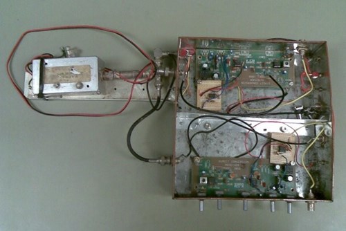
The original Simple Interferometer relied upon one of the receiver boards feeding its internally generated local oscillator to the other receiver board, thus providing a common local oscillator which is an essential component of this type of interferometer. This arrangement is fine for its intended application but the opportunity to implement a cleaner, more stable though somewhat more complex local oscillator has been made available to us.
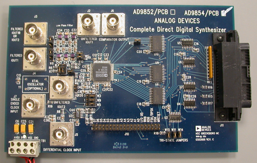
Analog Devices produce many direct digital synthesis devices, one of which is the AD9854. While there are many newer and more powerful DDS devices currently available, this choice of device is more than adequate for our purposes. In a nutshell, the AD9854 is a pair of programmable 12bit digital to analogue converters (DAC) with a maximum clock speed of 300MHz. The two DACs can be phase shifted by 90° to provide both incident and quadrature outputs up to a maximum frequency 150MHz, assuming we maintain the minimum Nyquist ratio of 2:1 . Practically, the device output frequency would be run up to about 120MHz. We have been able to obtain some blank printed wiring boards for the AD9854, based on a simplified version of the Analog Devices Evaluation Board that you can find details of here, including a tutorial and datasheets etc. There is a schematic for the simplified version of the evaluation board here and an image of the simplified board (blank) here. The AD9854 device is still available to buy at a moderate cost of about $40 per chip. Along with another $40 to $50 worth of components, some soldering and programming skills we end up with a frequency tunable, amplitude settable oscillator with a very respectable harmonic output and low phase noise figure.
DDS Output Filtering
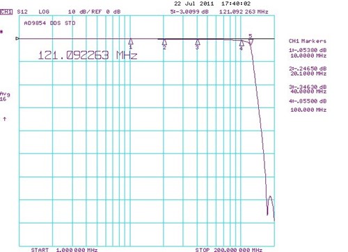
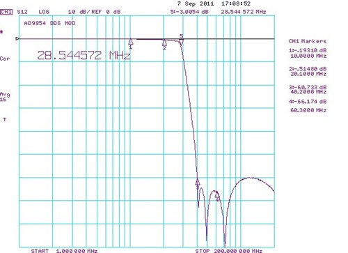
The original AD evaluation board and our simplified version were configured with 4 outputs, of which 2 are unfiltered and 2 have 7 element elliptic (cauer) low pass filters with a 3dB rolloff at about 120MHz.
For our application as an incident/quadrature local oscillator operating at an output frequency of 20.1MHz, a lower 3dB frequency of 25MHz has been selected and calculated using Elsie, an excellent Windoze program for filter design. There is a link to Elsie here. Short of leaving off the SMA connectors on the unfiltered outputs for cost reasons, all the headers, jumpers and connectors are fitted and available for testing purposes, if nothing else. There is a pdf parts list that includes easily obtainable component values suitable for the 25MHz low pass filter.
Driving the DDS
At this stage I have not yet powered up one of these items, but intend to very soon. For those following this page/activity and wish to take it further (before me) please read this information here. There is a very real danger that the levels of your PC digital output will destroy the AD 9854, which runs on a 3.3V rail and even a TTL signal easily exceeds this limit. Apart from the advice mentioned above, Jouni Verronen offers some free software that can be used to set the DDS output frequency, amplitude and other functions. Again, I stress that I have not yet tried this software and can only suggest it to you without any recommendation. For now, you are on your own.
Ten-Tec 1056 Direct Conversion Receiver
Tue, 08/02/2011 - 21:50 — peter
Out of the Box operation
(from the manual)
The efficient simplicity of this and similar receivers is made possible by the Signetics NE612AN mixer-oscillator U1, functionally identical to the well known NE602. The NE612AN is used because it is standard Ten-Tec inventory. L1, C1 & C2 form a tuned RF input circuit coupling the antenna to U1, Pins 1 & 2. The dissimilar values of C1 and C2 are selected for impedance matching . Potentiometer R1 is an attenuator to minimise overload by strong signals and nearby AM broadcasts, therefore serving as RF gain control. The local oscillator frequency is determined by C3, C4, L2 and the varactor tuning network coupled through C5. Voltage applied through tuning potentiometer R2 and R4 to the MV209 varactor provides coarse tuning or "band set". The fine tuning or "band spread" by R3 is done by coupling the control voltage to D1 through R5. As desired, changing the value of R5 will increase or decrease the fine-tuning rate.
Zener Diode D2 regulates the voltage to the oscillator's varactor circuit, supporting U1's never exceed Vcc limit of +8V.
The output from U1, Pins 4 & 5 is low level audio, the direct conversion result from mixing antenna RF input with the variable local oscillator frequency. This audio output is coupled through the filter network formed by R6 thru R9 and C10 to the inputs of U2a. The LM358 (U2 a,b) is a dual op-amp. The voltage gain from the antenna input to U1 through to U2a output is typically 68dB. The other LM-358 op-amp (U2b) and its associated components serve as an elementary bandpass filter, with front-panel filter tuning done by potentiometer R16.
Initially, the Ten-Tec 1056 will be used in its 'out of the box' configuration for Jupiter emission observations until sometime in 2013 when it will become part of another Simple Interferometer.
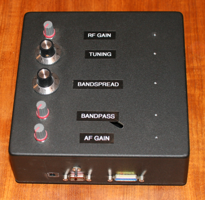
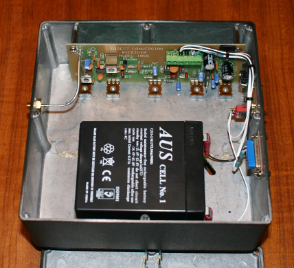
A single Ten-Tec 1056 receiver
For the interferometer, note that there is provision for another receiver to be fitted to this enclosure as indicated by the additional set of pilot holes for the controls on the enclosure's top panel. The battery will have to be relocated to another enclosure and it's capacity increased to drive the second receiver and the incident/quadrature local oscillator common to both receivers. The local oscillator will be one of the AD9854 Direct Digital Synthesiser boards detailed here. The local oscillator will be housed in another identical enclosure (3 in all), these diecast boxes should provide sufficient shielding to suppress any digital interference/noise away from the receiver's front ends.
For future operation, receiver sensitivity will be enhanced with a low noise amplifier, to be inserted between the RF line behind the divider/prior to the receiver. This LNA adds about 9.6dB gain at 20MHz, the additional gain may overcome the perceived lack of sensitivity for the Ten-Tec 1056 receiver noted in 2011.
It should also be noted that amplifiers often add more problems than they solve and they should be used with caution
to ensure that there is a tangible benefit obtained rather than just adding additional noise and interference.